


With the rapid development of the photoelectric industry, the semiconductor and other microelectronics industry has ushered in a golden age of development, which makes the performance and quality of products become the pursuit of microelectronics technology companies. High precision, high performance and high quality are the industry standards and enterprise product inspection standards in many high-tech fields. During the whole process of microelectronic packaging, various particles and other contaminants are attached to the surface of semiconductor devices. The existence of these pollutants will seriously affect the reliability and service life of microelectronic devices.
The quality of packaging process directly affects the output of microelectronic products, and the biggest problem in the whole packaging process is the pollutants attached to the surface of the product. Plasma cleaning can be applied to the front end of each process according to the different links of pollutants. It is distributed before pasting, lead bonding, and plastic packaging. The role of plasma cleaning in the whole packaging process mainly includes the prevention of packaging delamination, improving the quality of welding wire, improving the bonding strength, improving the reliability, improving the yield and saving the cost.
Dry cleaning has obvious advantages in many cleaning methods because it can remove contaminants without damaging the material properties and electrical conductivity of the chip surface. Among them, plasma cleaning has obvious advantages. It has the characteristics of simple operation, high control precision, no heat treatment, no pollution, safe and reliable. It has been widely used in the field of advanced packaging.
Principle of plasma cleaning technology
Plasma is a state of matter with sufficient positive and negative charge of charged particles in a colloid, or a non-condensed system consisting of a large number of charged particles. Plasma consists of molecules and atoms with positive and negative charges and metastable states.
On the one hand, when various active particles contact with the surface of the object to be cleaned, various active particles will react with impurities on the surface of the object to form volatile gases and other substances, which will then be sucked away by the vacuum pump. For example, reactive oxygen plasma reacts with organic matter on the surface of a material.
On the other hand, various active particles will bombard and clean the surface of the material, so that the contaminated impurities on the surface of the material are sucked away with the air flow by the vacuum pump. This cleaning method has no chemical reaction, and there is no oxide on the surface of the material after cleaning, so it can maintain the purity of the material after cleaning and ensure the anisotropy of the material.
(transistor shape), that is, transistor shape. Most early transistors used a coaxial package that was later borrowed for optical communication, called a package, i.e. Coaxial devices currently dominate the mainstream optical device market due to their ease of manufacture and cost advantages.
In the development and production of optoelectronic devices, packaging often accounts for 60% to 90% of the cost, of which 80% of the manufacturing cost comes from the assembly and packaging process. Therefore, packaging plays an important role in reducing the cost and has gradually become a research hotspot.
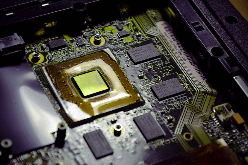
The problems in packaging mainly include welding layering, weak welding or insufficient bonding strength. The main culprit of these problems is the contaminants on the lead frame and chip surface, mainly including particulate pollution, oxide layer, organic residue, etc. These contaminants make the copper lead connections between the chip and the frame substrate incomplete or solder. How to solve the particulate oxide layer and other pollutants, improve the quality of packaging is particularly important.
Plasma cleaning technology mainly through the active plasma on the surface of the material physical bombardment or chemical reaction of single or double effect, in order to achieve the removal or modification of material surface pollutants at the molecular level. In the process of packaging, it can effectively remove organic residues, particulate pollution and thin oxide layer on the surface of materials, improve the surface activity of the workpiece, and avoid bonding delamination or virtual welding.
Plasma cleaning can not only greatly improve the bonding performance and bonding strength of the lead frame, but also avoid the secondary pollution caused by human factors contacting the lead frame for a long time.
After plasma cleaning, the result of product treatment is usually measured by drop Angle or Dyne value. The following figure is the comparison of water drop Angle before and after the plasma cleaning technology of a silicon photosensitive transistor.
According to the test data before and after the experimental cleaning, the contact Angle of the product surface decreased from 97.363° before cleaning to less than 10° after cleaning, indicating that the plasma cleaning method can effectively remove various impurities and pollutants on the product surface, thus improving the strength of material bonding and wiring. Effectively eliminate the layering in the subsequent chip packaging process.
The biggest advantage of plasma cleaning is that it can clean products of various sizes and structures without waste liquid and pollution sources.